Silicon and carbon nanostructures deposition (nanoCVD)
The laboratory of diamond layers and carbon nano-structures and laboratory of silicon layers and nanostructures.
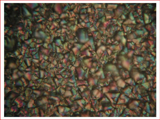
Core facilities of the Laboratory of diamond thin films and carbon nanostructures include of two unique microwave deposition systems. The microwave plasma CVD reactor with ellipsoidal cavity, i.e. focused plasma, is routinely used for growth of nanocrystalline diamond thin films (NCD) consisting of grains in size 20-200 nm. NCD films exhibit excellent optical and electronic properties that are good enough for the fabrication of various demonstrators as FET transistors or sensors, for example phosgene gas sensors.
The pulsed microwave plasma CVD reactor in configuration with linear antenna (installed 2008) is presently used for growth nano- and poly-crystalline diamond film over large areas. We observed that process parameters as gas mixture (i.e. mainly adding CO2 to the gas mixture CH4+H2) and process pressure (i.e. the range 6-100 Pa) controls not only the crystal size but also porosity of grown films. Presently, the deposition system is used for fundamental studies of plasma process and growth of diamond films for multi-disciplinary oriented fields as tissue engineering and regenerative medicine.
The laboratory of silicon films and nanostructures uses two plasma-enhanced CVD systems equipped with an RF power source working at 13.56 MHz and 40 MHz, respectivelly. The high-frequency PECVD system is used for the growth of amorphous and microcrystalline silicon films and nanostructures and silicon nanowires and for fabrication of silicon devices such as solar cells and diodes. The indurstrial-frequency PECVD is used for synthesis of silicon nanocrystals.
Equipment:
-
Microwave plasma CVD system with focused plasma (Aixtron)
-
Large area pulsed microwave plasma CVD system with linear antennas (Roth and Rau)
-
Reactive ion etching (Trion, Phantom LT)


